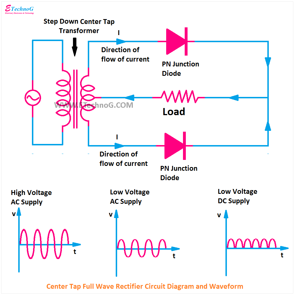
Full Wave Rectifier Schematic Diagram
Rectifier transformer tapped output waveform input Rectifier study Rectifier circuit diagram
Full Wave Bridge Rectifier - its Operation, Advantages & Disadvantages
Full wave bridge rectifier Schematic structure of the full-wave rectifier under study. Rectifier bridge wave circuit diagram diode voltage operation peak fig its shown below inverse value when negative
![Rectifier Circuit Diagram | Half Wave, Full Wave, Bridge - ETechnoG](https://1.bp.blogspot.com/-ph3wPcxTMhg/YO60L9F14dI/AAAAAAAABM0/svLo3j9BnrEtn4_4Ldv94ZgxqVJXvAE7ACLcBGAsYHQ/s1035/Center%2BTap%2BFull%2BWave%2BRectifier%2BCircuit%2BDiagram.png)
![Schematic structure of the full-wave rectifier under study. | Download](https://i2.wp.com/www.researchgate.net/profile/Ping_Li58/publication/262771370/figure/download/fig1/AS:614309948313609@1523474313391/Schematic-structure-of-the-full-wave-rectifier-under-study.png)
![Full Wave Bridge Rectifier - its Operation, Advantages & Disadvantages](https://i2.wp.com/circuitglobe.com/wp-content/uploads/2015/12/FULL-WAVE-BRIDGE-RECTIFIER-FIG-5-compressor.jpg)